Semiconductor packages used for artificial intelligence (AI) are getting large enough to push beyond some of the equipment and carriers traditionally used to manufacture them.
That growth is already changing how Intel Foundry moves products through its Fab 9 advanced packaging operation in Rio Rancho, New Mexico. The company has upgraded automated material handling systems to accommodate larger and heavier carriers, while also working with equipment manufacturers on expanded standards for package sizes that will exceed current tray formats.
The changes are being driven by advanced semiconductor designs that combine multiple specialized chips, or chiplets, into a single package for high-performance computing applications, including data centers.
Those larger packages are changing both equipment and automation capabilities.
“As the size of the package increases, it drives changes in the manufacturing equipment capable of making them,” said Tyler Osborn, director of advanced packaging technology development at Intel Foundry, in an interview.
Intel says its technologies can currently scale packages to eight times the industry-standard reticle limit, with plans to exceed 12 times that limit by 2028.
Larger packages drive equipment changes
Intel’s embedded multi-die interconnect bridge (EMIB) technology uses small silicon bridges embedded in the substrate to connect multiple chips within a package. As package sizes increase, some manufacturers are shifting how they process them.
“For example, larger integrated complexes are migrating from wafer-scale integration to panels for many companies,” said Osborn. “EMIB is already a panel-level process and is well positioned for this trend, but changes are needed in other parts of the assembly and test flow.”
Traditionally, semiconductor components have been carried through assembly in standardized trays developed under the Joint Electron Device Engineering Council (JEDEC), an industry organization that establishes semiconductor standards.
“These new package sizes will exceed what can be carried in current tray formats,” said Osborn.
Intel is working with equipment manufacturers on expanded standards for those larger formats. Osborn said the company has also upgraded its automated material handling systems (AMHS), which move products throughout the factory.
“As package sizes have grown, we’ve upgraded these systems to handle larger and heavier carriers than those used in a traditional 300mm wafer fab,” he said. “That includes higher-capacity vehicles and transport systems, as well as new carrier designs, to safely move products through the factory while maintaining highly automated manufacturing operations.”
But size is only part of the challenge.
“Some of the more significant challenges arise in handling the weight, warpage, and uniformity of these large processing sizes,” said Osborn.
He said those factors create new requirements for equipment that must move and process products while maintaining the precision required in semiconductor manufacturing.
Automation links the process
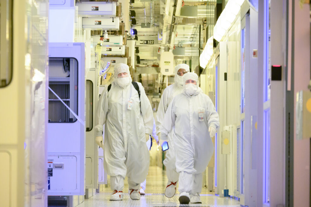
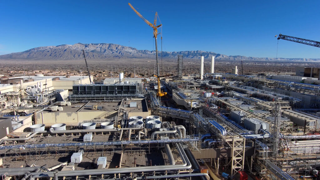
Osborn explained that Fab 9 is one of Intel’s largest wafer assembly high-volume manufacturing facilities, and that automation plays a major role in operations.
“It utilizes fully automated delivery of wafers and shop floor controls very similar to a standard 300mm wafer fab,” said Osborn. “Virtually everything is processed and moved from tool to tool with automation and robotics.”
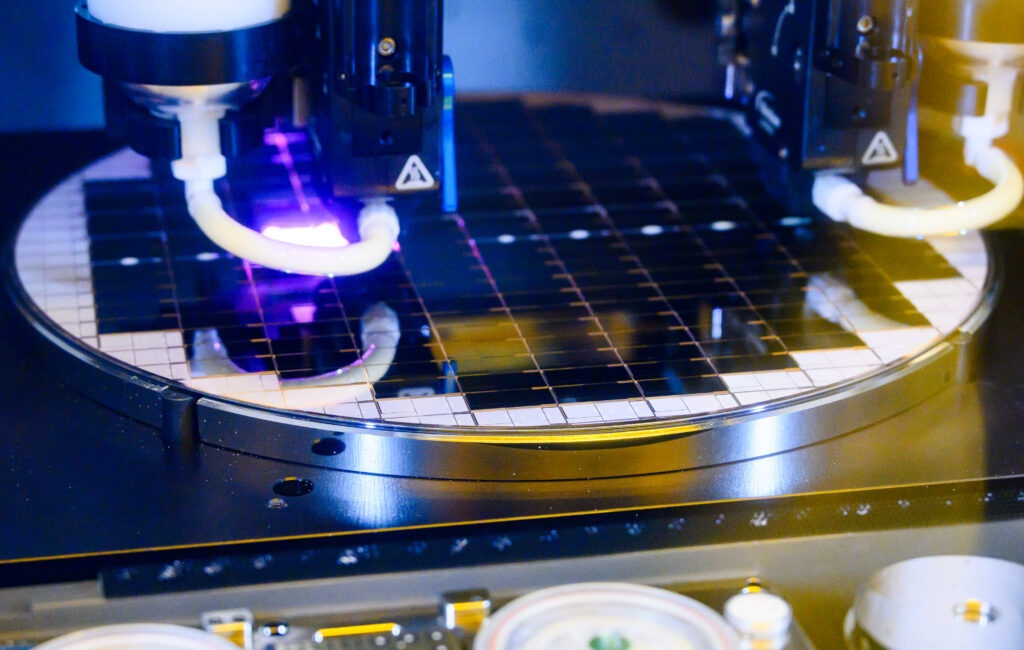
That manufacturing capability can be seen throughout Foveros, Intel’s proprietary advanced chip packaging process. Foveros connects smaller chiplets on a silicon interposer, which Intel describes as similar to a pizza crust, with the individual chiplets acting as toppings.
A chip attach tool places the chiplets on the wafer before it is heated. An overhead robotic track system moves front-opening unified pods (FOUPs) carrying wafers between equipment, including a machine that applies epoxy beneath and around the chiplets. Water-cooled blades eventually dice the wafer into individual packages.
Inspection takes on a bigger role
As more computing capability is built into each package, Osborn explained that quality becomes even more important.
“Process complexity and density of compute are driving yield and quality to be more and more important in packaging, similar to the challenges that arose in transistor fabrication decades ago,” he said.
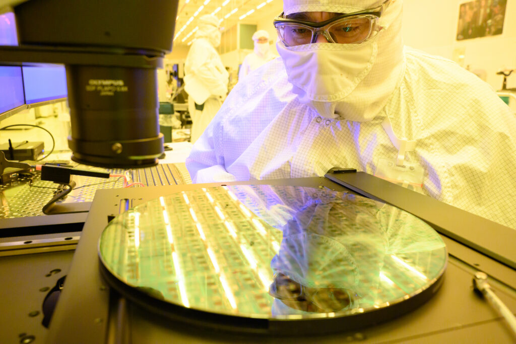
Intel uses inspections, automated vision systems, and multiple types of sensors throughout its assembly process to help maintain both quality and yield.
The equipment also must support different combinations of chiplets and technologies. According to Intel, Foveros allows different chips built on different designs or technology nodes to be combined on the same wafer.
“Flexibility is critical as the desire for heterogeneous integration continues to evolve,” said Osborn. “Packaging different chiplet combinations and technologies is critical to supporting the designs our customers need for their specific use cases.”
Where automation goes next
Even with the high level of automation already deployed inside Fab 9, Intel sees opportunities to automate more of the process.
“There are many opportunities in packaging to continue advancing automation,” Osborn said. “In particular, material movement in and out of the factory and consumable material replacement are areas with opportunities for innovation.”
But one of the biggest challenges may be keeping equipment development moving quickly enough as semiconductor packages continue to grow.
Osborne notes that as package sizes increase, having equipment capable of supporting ever larger form factors remains a major challenge. “Equipment development requires significant time and investment from equipment manufacturers.”
The challenge will require coordination beyond Intel’s own factories.
“Continued innovation across the industry, combined with greater standardization where appropriate, can help accelerate adoption and improve efficiency while enabling differentiated packaging solutions,” said Osborn.